TSMC CoWoS vs. Intel Foveros: Two Bets on the Same Future
 P. Nakamura
TSMC and Intel agree that advanced packaging is the next battleground. They disagree on almost everything else. Their competing approaches -- CoWoS and Foveros -- represent genuinely different architectural bets with different tradeoff curves.
TSMC's CoWoS (Chip-on-Wafer-on-Substrate) is a 2.5D approach. Chiplets sit side-by-side on a silicon interposer that provides high-density interconnects between them. The interposer acts as a communication highway -- dense enough for HBM integration, wide enough for massive bandwidth between compute and memory. CoWoS-S uses a full silicon interposer. CoWoS-L uses a combination of local silicon interconnects and an organic substrate to reach larger package sizes without an enormous (and expensive) monolithic interposer.
NVIDIA's dependency on CoWoS for its GPU packaging is well documented. The H100 and B100 both use CoWoS, and TSMC's CoWoS capacity has been a genuine bottleneck for the AI hardware supply chain. When your packaging capacity constrains how fast the most valuable chips in the world can ship, you know the technology matters.
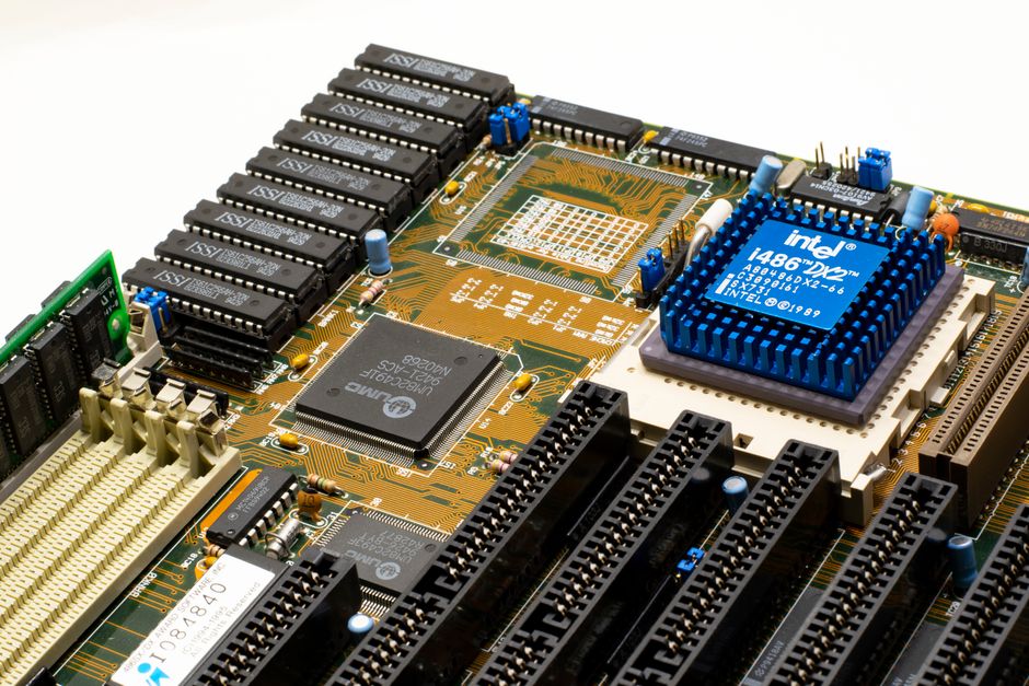
Intel's Foveros is a 3D approach. Chiplets stack vertically, with through-silicon vias (TSVs) connecting active die layers. This is architecturally more aggressive -- you get shorter interconnects, higher bandwidth density, and a smaller package footprint. Intel has used Foveros in Lakefield and Meteor Lake, stacking compute tiles on top of base tiles that handle IO and connectivity.
The tradeoffs are real. 2.5D packaging (CoWoS) is more thermally forgiving because chiplets are spread laterally and heat dissipation paths are more straightforward. 3D stacking (Foveros) puts heat sources on top of each other, creating thermal challenges that require careful power management and sometimes exotic cooling solutions. But 3D stacking enables tighter integration and shorter wire lengths, which translates directly to lower latency and power consumption for inter-chiplet communication.
Capacity is the other dimension. TSMC is spending billions expanding CoWoS production. Intel is investing in both Foveros and its EMIB (Embedded Multi-die Interconnect Bridge) technology, which is a more targeted 2.5D approach connecting specific pairs of chiplets rather than using a full interposer.
Neither approach wins universally. High-bandwidth compute-to-memory applications favor 2.5D today. Tightly coupled heterogeneous compute may favor 3D tomorrow. The market is big enough for both, and the real winners will be the companies that understand which architecture fits which workload.
Get Chiplet Ecosystem in your inbox
New posts delivered directly. No spam.
No spam. Unsubscribe anytime.