Why Chiplet Disaggregation Makes Power Domain Isolation a First-Order Packaging Problem
 P. Nakamura
Power domain isolation used to be a job for the RTL team. Define your voltage islands, drop in level shifters, add isolation cells at the boundary, and move on. Single-die designs gave you the luxury of solving this problem entirely in silicon, with the package as a passive bystander.
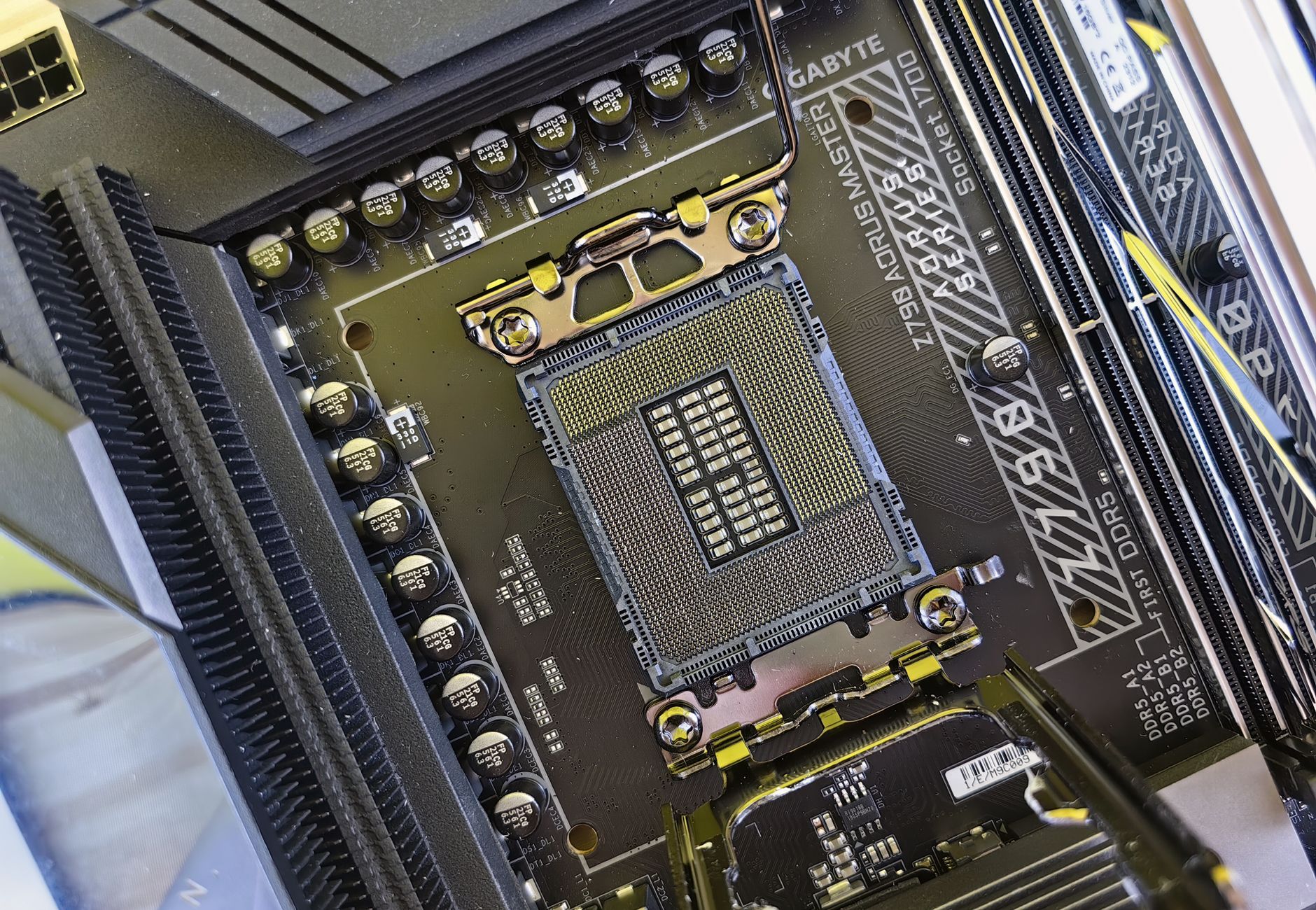 Photo by Andrey Matveev on Pexels.
Chiplet disaggregation ends that arrangement.
When you split a design across multiple dies, each potentially fabbed at a different node by a different foundry, the boundaries between power domains stop being logical constructs inside one piece of silicon. They become physical gaps between separate dies, separated by bump arrays, redistribution layers, or hybrid bond pads. The package substrate is now load-bearing infrastructure for your power delivery scheme, and the decisions get locked in long before any RTL synthesis runs.
Here is what actually changes. On a monolithic die, a level shifter sits a few microns from the logic it serves. Propagation delay is negligible, and the shifter draws power from whichever rail is convenient. Disaggregate that same boundary across two chiplets, and your level-shifting function either moves into the die-to-die interface logic (consuming area in your SerDes or UCIe PHY) or it lands on the package substrate itself as a discrete or embedded component. Neither option is free.
The more insidious problem is ground referencing. Two chiplets with separate power delivery networks will, under realistic load conditions, develop a voltage differential between their respective VSS planes. On a monolithic die, VSS is VSS: a shared copper grid that equalizes potential across the whole die. Package-level integration connects chiplet grounds through the substrate stackup, through microbumps or C4 bumps, through a path that carries real inductance and resistance. Under a transient load on one chiplet, its local VSS bounces. The neighboring chiplet's I/O receivers see that bounce as signal noise on any wire that crosses the domain boundary.
graph TD
    A[Chiplet A: 3nm Logic] --> B(UCIe PHY / D2D Interface)
    C[Chiplet B: 7nm I/O] --> B
    B --> D[Package Substrate RDL]
    D --> E{Split Power Delivery}
    E --> F[VDD Rail A: 0.75V]
    E --> G[VDD Rail B: 1.0V]
    F --> A
    G --> C
Package engineers deal with this through deliberate VSS stitching: adding dedicated ground bumps along the die-to-die boundary at a density high enough to keep impedance below the threshold where noise coupling becomes a signal integrity problem. The exact density depends on the transient current profiles of both dies, which means the power delivery network co-design has to happen before bump map allocation is finalized. That sequence matters. You cannot place bumps after the substrate is routed.
Voltage regulators add another layer of coordination. Integrated voltage regulators (IVRs) inside a chiplet regulate their own rails, but they introduce switching noise at their operating frequency. When two chiplets with different IVR designs sit millimeters apart on an organic substrate, their switching noise couples through the substrate. The coupling magnitude depends on the substrate's dielectric constant and the spatial distance between the regulators' output capacitors. A silicon interposer attenuates this coupling better than an organic substrate, which is one concrete reason some power-sensitive designs pay the cost premium for silicon-based integration.
On-package decoupling capacitor placement becomes a co-optimization problem that spans both the mechanical floorplan and the electrical model. A decap placed too close to a chiplet boundary can inadvertently couple noise from one domain into another if the substrate routing connects them to the wrong net. Placed correctly, with explicit keepout rules around the domain boundary, it suppresses rail bounce before it propagates.
What does this mean for design teams? The power architect has to be in the room when the package substrate stackup is being chosen. Not reviewing the substrate decision afterward; actually influencing it. The number of power and ground layers in the substrate, the via density, the dielectric stack: all of these set the PDN impedance that the power domains will have to coexist within.
Some teams handle this by treating the entire package as a single PDN simulation domain from the start, combining chiplet-level SPICE models with substrate parasitic extraction before any sign-off on the physical partition boundaries. It is more work upfront. It reliably avoids the situation where two teams build their pieces independently and discover a ground bounce problem during bring-up, when the substrate is already built and the chiplets are already taped out.
Disaggregation trades one hard problem for several distributed ones. Power domain isolation happens to be the one that bites hardest when the teams do not talk to each other early enough.
Get Chiplet Ecosystem in your inbox
New posts delivered directly. No spam.
No spam. Unsubscribe anytime.