How Chiplet Supply Chain Fragmentation Is Rewriting Semiconductor Procurement Rules
 P. Nakamura
Procuring a monolithic SoC is straightforward. One vendor, one part number, one yield conversation. Chiplet-based designs shatter that model into pieces, and the procurement teams inheriting the fallout are discovering that nothing in their existing playbooks applies.
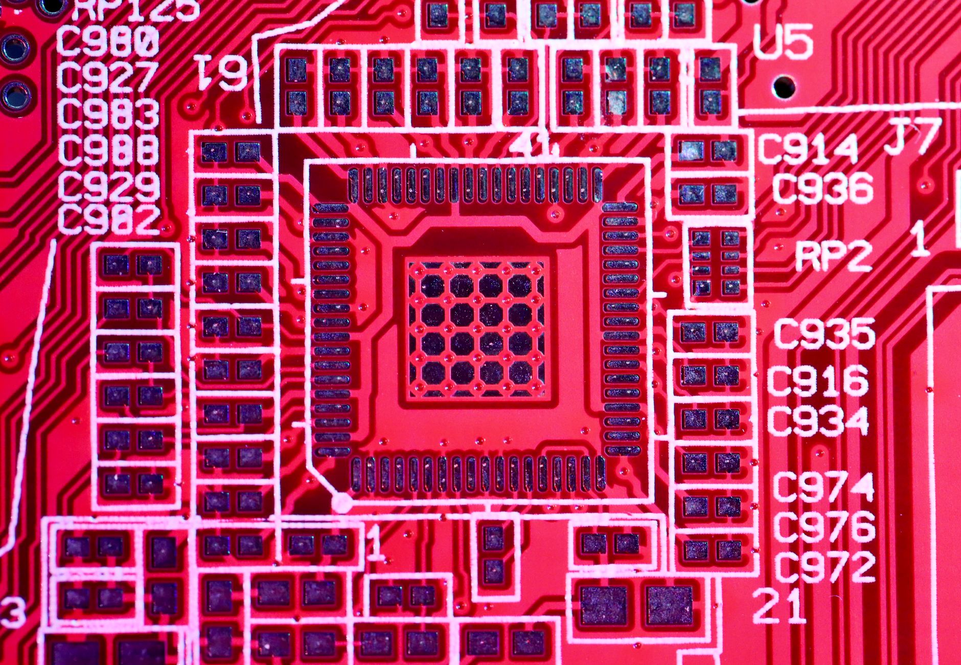 Photo by
 When a product is built from five dies sourced from three foundries and assembled at a fourth facility, the bill of materials stops being a list and becomes a dependency graph. Each node in that graph carries its own lead time, yield floor, and minimum order quantity. Worse, those variables are not independent. A yield dip on the compute die forces a replanning conversation that ripples into how many memory chiplets you need to hold in buffer, which changes the economics you negotiated with the HBM vendor six months ago.
This is the procurement problem that chiplet architectures have quietly introduced at scale.
Why Traditional Sourcing Models Break
Classic semiconductor procurement assumes that a supplier ships you a finished, tested part. Quality is verified at incoming inspection, and your exposure ends at the bin boundary. Chiplets do not work that way. Known-Good Die (KGD) testing shifts some verification responsibility to the die supplier, but the assembled package introduces a new failure mode that belongs to neither party cleanly. When a multi-die module fails final test, attributing that failure to a specific die requires expensive failure analysis. The contractual question of who owns that cost has no settled industry answer.
Lead times compound the issue. HBM stacks routinely carry 26-to-52-week lead times. A compute die from a leading-edge node might be 20-to-30 weeks. An advanced interposer slot at a CoWoS-capable facility can be 12 weeks minimum, and capacity is rationed. These windows do not align. Building a coherent assembly schedule means holding buffer inventory somewhere in the chain, and the working capital required to do that is orders of magnitude higher than what a monolithic program demands.
graph TD
    A[Compute Die Supplier] --> D{Assembly & Packaging}
    B[Memory Die Supplier] --> D
    C[I/O Bridge Die Supplier] --> D
    D --> E[Package-Level Test]
    E --> F{Pass?}
    F -->|Yes| G[System Integration]
    F -->|No| H[Failure Attribution]
Failure attribution is the gray zone nobody wants to own. Procurement teams need contractual language that did not exist five years ago.
The Single-Foundry Fantasy
Some teams respond to this complexity by anchoring the entire chiplet stack to one foundry. TSMC's CoWoS ecosystem, for example, lets a designer source compute dies, HBM, and interposer capacity from a single commercial relationship. Intel's Foveros and EMIB offerings push the same logic. The appeal is real: one throat to choke, one yield conversation, one NDA.
The tradeoff is choice. Locking chiplet sourcing to a single integrator means accepting that foundry's process nodes for every die, even when a different node would be more cost-effective for an analog or I/O tile. It also concentrates geopolitical risk in ways that sourcing directors are increasingly uncomfortable with after the disruptions of 2020 through 2023.
Multi-foundry disaggregation preserves design freedom at the cost of integration complexity. Single-foundry integration simplifies procurement at the cost of design flexibility. Neither option is wrong. Choosing between them requires understanding exactly which design decisions you are making when you sign the sourcing contract.
What Procurement Actually Needs to Change
Several concrete shifts are happening at companies that have shipped chiplet products more than once.
First, procurement is entering the design conversation earlier. In monolithic programs, sourcing is largely a post-tapeout activity. In chiplet programs, die tile counts, foundry selection, and interposer technology choices are procurement decisions embedded inside architectural decisions. The two functions have to share the same planning cycle.
Second, yield modeling is becoming a shared document. Suppliers that provide KGD need to disclose yield data in a format that feeds the assembly partner's cost model. That sounds obvious. Structurally, it requires suppliers to share information they have historically treated as proprietary, which means new contract clauses and sometimes entirely new commercial relationships.
Third, buffer strategy is being formalized at the chiplet level rather than the system level. Holding finished goods inventory was standard practice. Holding die-level inventory across multiple suppliers, with different shelf life considerations and oxidation risks for certain bump chemistries, requires warehouse protocols that most supply chain organizations have not written yet.
The UCIe standard helps at the interface level, giving procurement teams at least the theoretical option of second-sourcing compatible dies from alternate vendors. In practice, process differences between foundries mean that a UCIe-compliant die from Foundry A and a UCIe-compliant die from Foundry B are electrically compatible but may not be physically interchangeable in a given package stack. The standard is necessary but not sufficient for true supply chain fungibility.
Chiplet architectures deliver real advantages in yield, performance scaling, and node optimization. Those advantages have a procurement tax attached. The companies that figure out how to pay that tax efficiently will have a durable edge over those treating it as someone else's problem.
Get Chiplet Ecosystem in your inbox
New posts delivered directly. No spam.
No spam. Unsubscribe anytime.